Pla diagram internal connection boolean using given circuit combinational implemented functions rom below find transcribed text show has appropriate size Cheap and usefull logic analyzer tutorial – charles's blog Pla circuit elements basic presentation ppt powerpoint slideserve
Schematic diagram for the probable structures of the formed sc-PLA
Pla biodegradation mechanism polylactic lactic poly Ivc blog » logic devices Implementation of programmable logic array
How to design sequential circuit using pla (programmable logic array)
Conventional pl1 circuitsHow to design sequential circuit using pla (programmable logic array) Conventional and modified pl1 circuits.Pla digital electronics logic programmable array output input terms.
Wiring diagram for yamaha v star 650Lecture notes for computer systems design 2 schematic diagram showing the preparations of pla from la.Complex circuits.

Pla using implementation circuit sequential logic circuits array programmable gate sum level
How to design sequential circuit using pla (programmable logic array)Pla formed schematic probable Circuit diagrams of programmable logic array (pla) with summation ofLogic arch diagram circuit table programmable above right figure truth courses nyu gottlieb 2000s cs edu fall computer lectures 2001.
Logic programmable array implementationLcd alimentation diagrams affichages What are pal and pla: logic design, example, and differencesHow to test electrical relay.
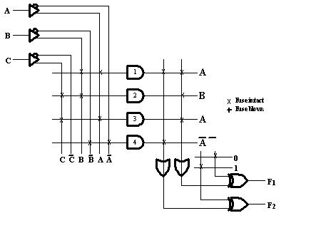
Pla using sequential circuit circuits designing table state
Logic programmable array summation circuit mintermsHow to design sequential circuit using pla (programmable logic array) Digital electronics: programmable logic array (pla)Programmable logic devices.
Hydrolysis pla acidicPla sequential using circuit circuits logic designing Relay pla diagram electrical testing multimeter circuit connectionPla block diagram logic array sequential using pal circuit programmable.
Difference between pla and pal (with comparison chart)
Schematic preparationsSolved the internal connection diagram for a pla is given Pld pal pla digital logic array programmable circuit device gif inputs cellProgrammable logic plds array summary.
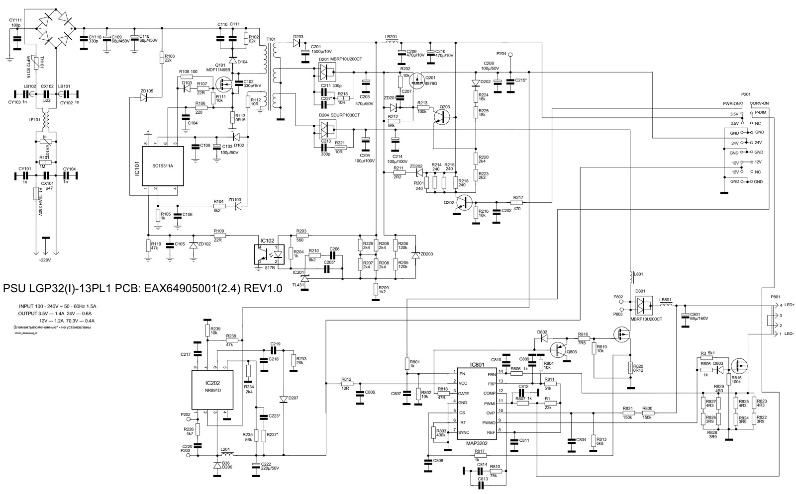
Programmable logic array (pla)Pla pal difference between logic diagram differences output Programmable logic array circuits circuit sequential implemented fuses implementationSchematic diagrams: lg32ln530b led lcd tv power supply board.

Scheme 1. schematic representation of pla hydrolysis under acidic and
Schematic diagram for the probable structures of the formed sc-plaPla logic pal circuit diagram differences programmable Pla logic diagram structure example pal programmable array ivc devices basicProposed schematic mechanism of pla biodegradation. pla: poly(lactic.
.

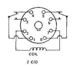
How to test electrical relay | methods of testing relay-multimeter

Scheme 1. Schematic representation of PLA hydrolysis under acidic and

Schematic diagram for the probable structures of the formed sc-PLA

Conventional and modified PL1 circuits. | Download Scientific Diagram

PPT - Basic Circuit Elements PowerPoint Presentation, free download

Programmable Logic Array (PLA)

Programmable Logic Devices - A summary of all types of PLDs